
A common question I get when discussing solar photovoltaic (PV) power is: “What is the typical efficiency for panels now?” When I answer that mass-market polycrystalline panels are typically about 15–16%, I often see the questioner’s nose wrinkle, followed by dismissive mumbling that 15% is still too low, and maybe they’ll wait for higher numbers before personally pursuing solar. By the end of this post, you will understand why this response is annoying to me. At 15%, we’re in great shape: it’s plenty good for our needs. Let’s do the math and fight the snobbery.
 A close-up of a polycrystalline photovoltaic (PV) cell, showing blue tint and a patchwork of crystal domains.
First, let’s look at the efficiencies of other familiar uses of energy to put PV into perspective. I will act as if I’m directly addressing the PV efficiency snob, because it’s fun—and I would never be this rude in person. This may not apply to you, the reader, so please take the truculent tone in stride.
Snark Attack
So 15% is far too low for you? Perhaps you reason that laboratory prototypes and expensive spacecraft applications can get 40%-plus results, so let’s not take the plunge prematurely, given the abysmal 15%.
Perhaps you drive a car. Maybe you’ll stop when you realize that it converts thermal energy from burning gasoline into locomotive power at an efficiency around 15–25% (and this on a finite resource). We should wait for better.
Electric cars deliver battery-stored energy to the wheels at something like 85% efficiency. Now we’re talking. But the charging process imposes another 85% efficiency, and the real kicker is that the fossil fuel (or nuclear) plant supplying the electrical power is only 35% efficient for a net fossil-to-wheels efficiency around 25% (same ballpark as the gasoline car).
Hydrogen fuel cells offer no efficiency advantage in practice, achieving 20–40% for the round-trip hydrogen conversions, not including the efficiency of creating and delivering the electrical power to drive the formation of hydrogen.
If you’re low on energy, you might consider eating. But on second thought, our metabolic efficiency of converting chemical energy into mechanical output is similar to that of a car, so why bother? Turn up your nose.
Perhaps you are a fan of biofuels. This is perhaps the best apples-to-apples comparison to PV, being solar-driven. An Iowa corn field captures solar energy at a paltry efficiency of 1.5%! Okay, but we know by now that corn ethanol has a number of problems. Algae can be far more efficient, right? But even here, photosynthesis tops out at something like 5–6% efficiency under ideal conditions.
PV is Actually Rather Remarkable
Considering this last point, I think it’s rather impressive that we beat biology by a factor of 3 in just a few decades of effort (biology had much longer to work on the problem). Moreover, 15% is perfectly adequate for our needs, as we’ll see at the end.
Qualitative assessments aside, it is rewarding to understand the origin of PV efficiency, and to appreciate that we’re not terribly far from the theoretical limit. The point is that we shouldn’t hold out for some arbitrary efficiency before we embrace solar PV: we don’t really need the extra efficiency, and in any case, physics has something to say about how high we might expect to go.
PV Basics
A photovoltaic cell is most typically a slice of crystalline silicon 200—300 μm thick. (μm = micron = micro-meter = one-millionth of a meter). The construction can either be monocrystalline—slowly grown from a large single-crystal boule, or polycrystalline, cast in an ingot and with a patchwork of crystal domains in varying orientations (translation: pretty to look at). Monocrystalline varieties have a slight advantage in efficiency: like 18% vs. 15%. The cell is doped into what we call a p-n junction, which is basically a diode. What is important here is that the junction is very near the front surface of the cell, and it is here that energy is effectively harvested.
It works like this: a photon of light comes in from the sky, penetrating some depth into the silicon. If it has enough energy (imagine a sign out front: “you must be this tall to go on this ride”), it can pop an electron out of the lattice, leaving a “hole” behind.
The Big Hit: Spectral Limit
This is all we need to know to take our first stab at an efficiency expectation. The first piece of knowledge is that photons below a certain energy cutoff called the bandgap energy (1.12 eV in silicon; corresponding to a wavelength of 1.1 μm) are not absorbed by the material: they sail right through as if going through clear glass. Second, the photons that are absorbed only need to have 1.12 eV of energy to liberate an electron out of the lattice. Any extra is wasted, popping the electron out at high speed. It rattles around the lattice, depositing its “sugar-high” as heat as it calms down.
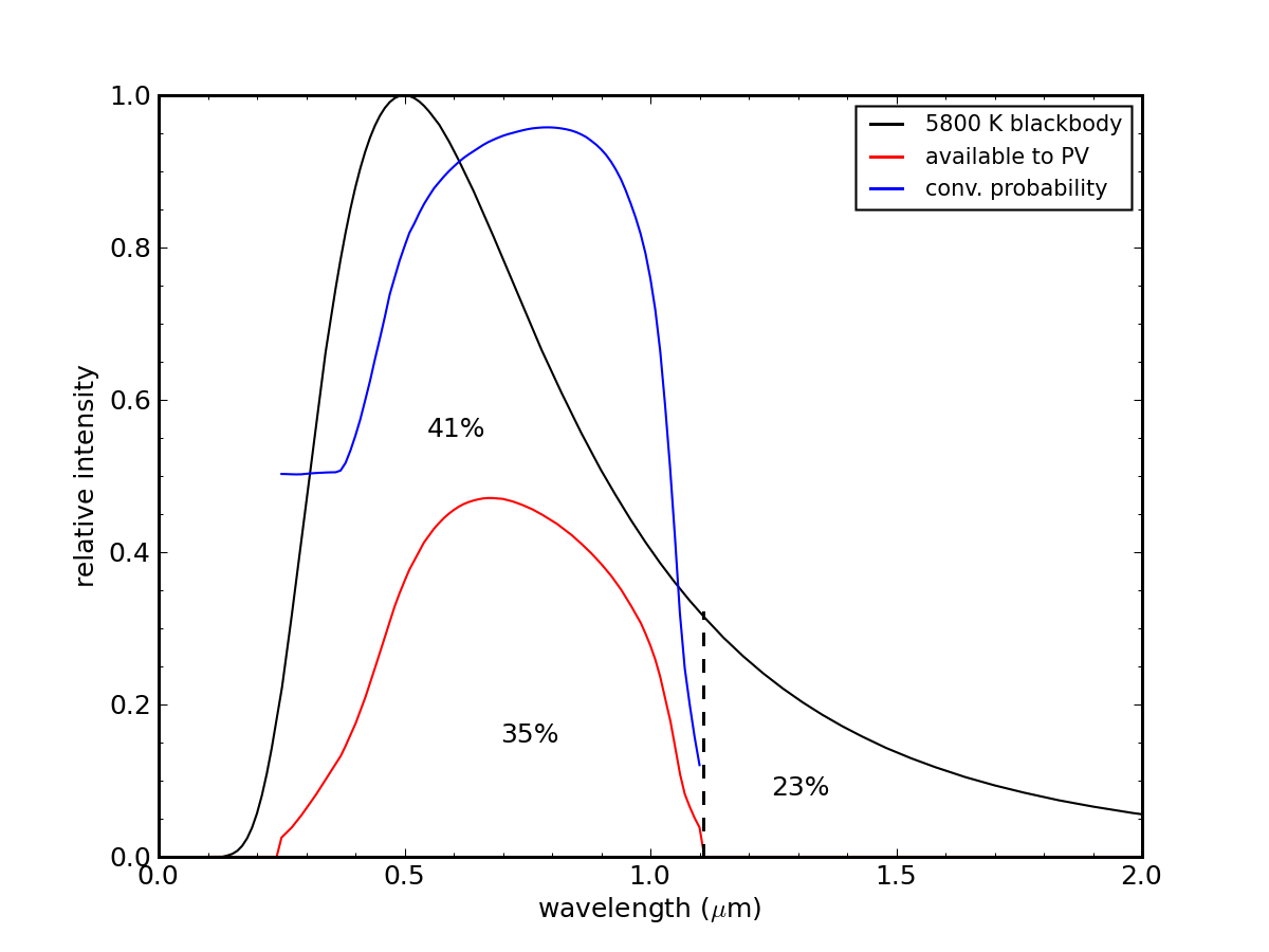
Putting these together, we can say that if a perfect blackbody solar spectrum is incident on the PV cell (ignoring atmospheric effects on spectrum), we lose 23% of the light to infrared transparency beyond 1.1 μm, plus a thermal loss that increases with increasing photon energy (shorter wavelength). The net effect is that we get to keep 44% for PV energy production. This ignores many other real physical limitations that we’ll address below, but it at least represents an upper limit to efficiency expectations.
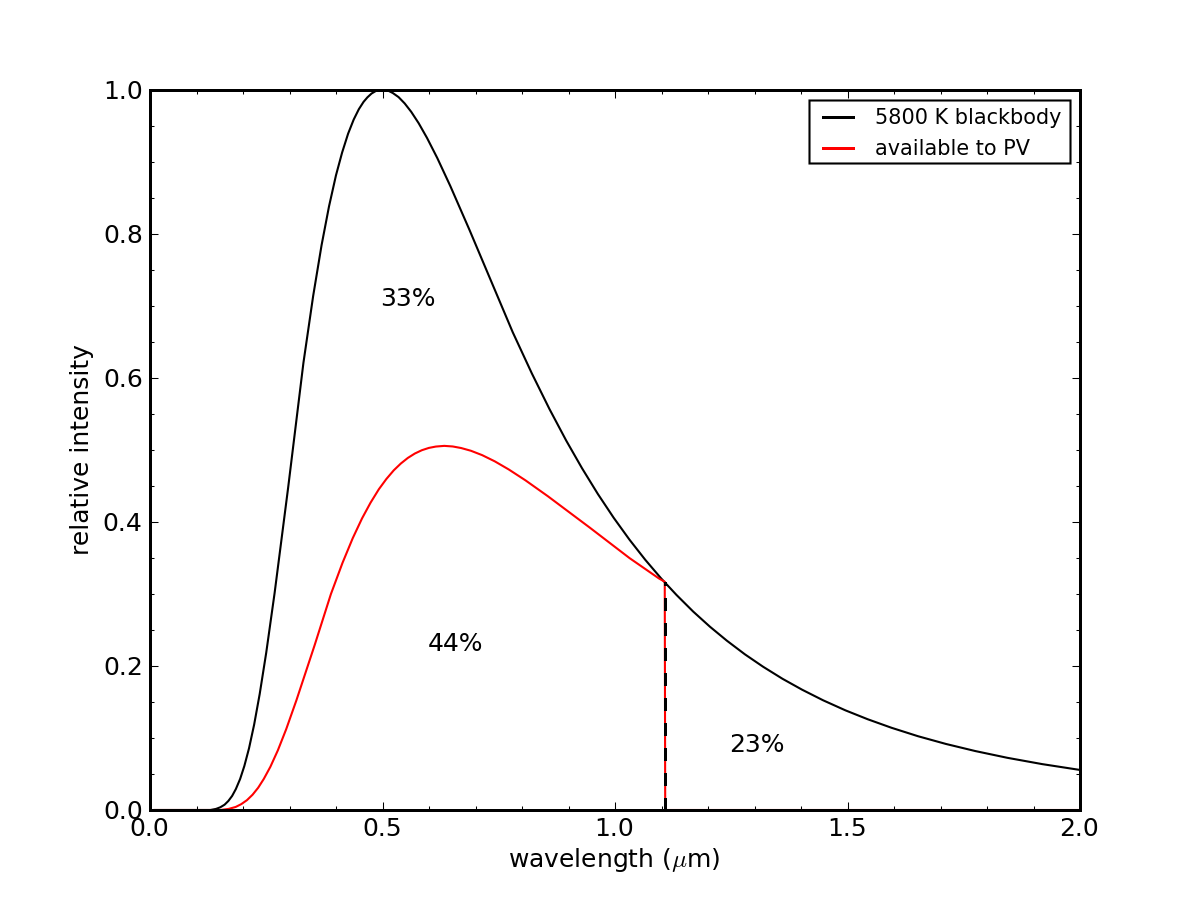
Considering only photon energy effects, a silicon PV cell ignores 23% of the incoming energy, and wastes 33% in light that arrives with more energy than can be utilized, leaving at most 44% available.
We see these effects in the figure above. At 1.1 μm, the photon is well-matched to the necessary energy for liberating an electron, and we use 100% of its energy. As we go to shorter wavelengths, a smaller fraction of the photon energy is utilized, resulting in 33% of the incident energy going to waste heat.
So this most basic analysis indicates that we are doing reasonably well to capture 16% efficiency out of a silicon PV cell when the crudely-determined upper limit is 44%. This is not much different from cars or power plants, in terms of how far below the theoretical thermodynamic limit we achieve in practice.
Better than Silicon?
As an aside, the bandgap energy of silicon is 1.12 eV, corresponding to a wavelength of 1.1 μm. Other semiconductor materials have different bandgap energies. Why restrict ourselves to silicon—even though it is very abundant and we benefit from substantial knowledge and experience via the computer chip industry and related enterprises? I was curious to know what would happen to our 44% theoretical efficiency calculation if we allow ourselves to pick any bandgap.
If we decrease the bandgap wavelength, we squander more infrared light, but use the visible-light-dominated portion of the solar spectrum more efficiently. Longer wavelength bandgaps mean more photons are available, but achieving lower efficiency at visible wavelengths. Where is the balance?
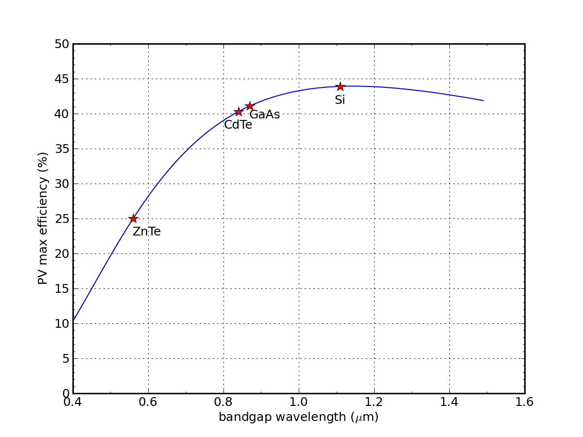
Considering only spectral losses, silicon sits near the maximum possible efficiency, compared to other common PV materials.
I was amazed to see silicon perched near the maximum efficiency position in this trade-off. Who knew? A more careful treatment—using the spectrum as received on the ground and effects like those explored below—finds the peak performance closer to 0.9 μm (1.38 eV), at around 34%.
Into the Weeds: Other Pernicious Limitations
A word of warning: we’re about to get into the nitty-gritty here, so if you’re already feeling a little queasy, there won’t be much harm in skipping to the last paragraph in this section.
Thus far, we have only considered the effects of the input spectrum for a single-bandgap device. But other physical limitations are at play, relating to where (or if) the photon is absorbed, the path history of the generated electron and hole, surface effects, etc. Here are four effects to consider (not a complete list):
- The expected penetration depth of the photon into the silicon depends on wavelength/energy. Photons near the bandgap can travel a very long way before being absorbed, while high-energy photons are absorbed practically at the front surface.
- PV cells are often fabricated with a reflective back surface (also acts as the electrode), so that photons passing through the entire wafer still have a chance to be absorbed on the rebound trip. The reflective barrier also reduces heating from infrared light that otherwise would be absorbed at the back of the cell.
- The p-n junction is at a finite depth, so the photons absorbed above this are far more vulnerable to surface loss.
- Shorter wavelength light suffers more reflection loss at the front surface than longer wavelengths, which is what often gives a blue tint to PV cells.
Absorption length (data from this site) is shown in the logarithmic plot below. This is only the characteristic depth of absorption, but the profile at any given wavelength follows an exponentially decaying probability of absorption, set by this scale.
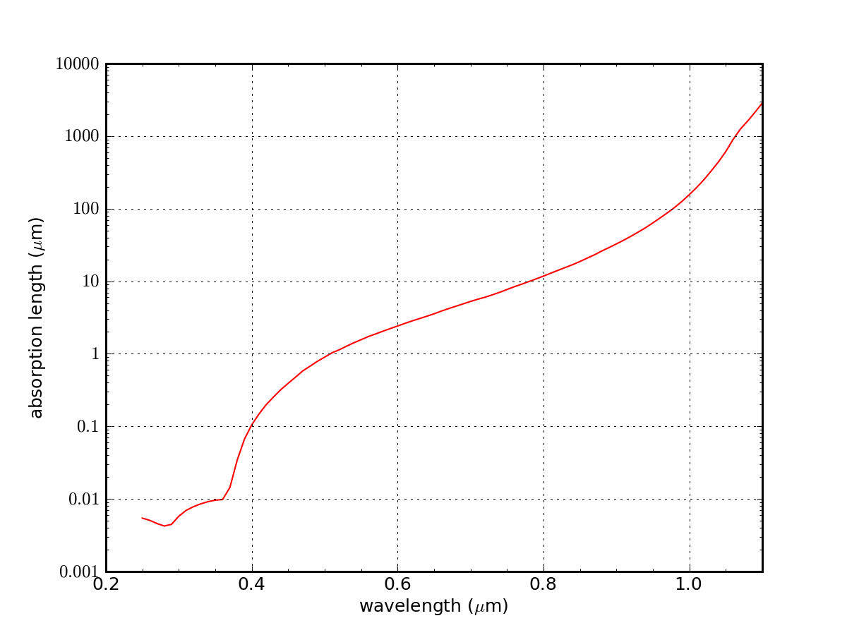
Logarithmic plot of the absorption length in silicon as a function of wavelength.
At a wavelength of about 0.5 μm (green light), the absorption length is about 1 μm. Shortward of this, the third effect enumerated above becomes important. Longward of a wavelength of 1.0 μm, the absorption length becomes > 200 μm, and the light often reaches the back surface, where factor 2 comes into play.
After the absorbed photon creates an electron-hole pair, the electron wanders about, bumping this way and that, with no direction in life (diffusion). If it happens to run into the p-n junction near the front surface, it gets swept across toward the front, where it joins a flock of eager electrons itching to run out into an external circuit and do some work. If it wanders off the other way (deeper into the crystal) it may never find the junction; eventually re-combining with a “hole” elsewhere—often facilitated by crystal grain boundaries and surfaces, or by defects and impurities in the crystal.
Likewise, a hole generated above the junction may wander into the junction and be pushed to the back, in an arranged marriage (recombination) with an electron returning to the back side of the cell from service in the external circuit. The junction therefore acts like a pump, pushing electrons one way and holes the other—encouraging them to participate in a flow of current through an external device.
I made a simple model to account for these effects, where the probability of being “pumped” is unity at the junction, tapering linearly to some lesser probability at the front and back surfaces (pf and pb, respectively). Linear makes some sense, because—as I had to prove to myself via simulation—the chance of a random walk bumping into one extreme or the other is just linearly proportional to its starting position relative to these two boundaries. If the junction always sweeps the charge, cashing in its energy, while the surface has some fixed probability of gobbling up the charge and thus forfeiting the energy, the probability relation for points between is linear. This ignores internal recombination along the way, which dis-favors long-haul paths, making the back surface “hungrier.”
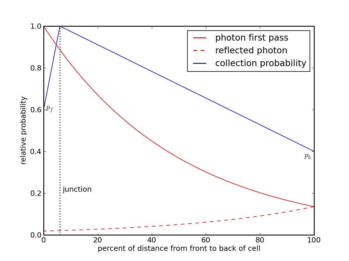
Model for evaluating conversion probability as a function of depth and penetration, ignoring bulk recombination losses. For a given wavelength, the absorption curve (red) is multiplied by the collection probability (blue) and integrated through the bulk. The front and rear surfaces have some probability of gobbling charge carriers that bump into them. The junction is actually much closer to the front, but is set back a bit for clarity
Folding this effect together with the exponential absorption probability vs. depth, and allowing perfect reflection at the back, I can produce an expectation that accounts for the first three factors above. I don’t explicitly cover the front-surface reflection loss. Most new photovoltaics have an anti-reflection coating that reduces what would be a 30% surface reflection to just a few percent across most of the visible and near-IR band. But it gives out at the blue or near-ultraviolet end, allowing the reflection to creep back up to 30%. Since the PV response at the blue end is weak already due to surface losses and poor utilization of photon energy, I just absorb the extra reflection loss into the front-surface gobble probability, which is relevant primarily for short wavelengths because of their tiny penetration depths.
Okay—boy are we in the weeds here: let’s try to pull out. Putting these effects together, we get an expected efficiency of a silicon PV of 35%: not far off from other evaluations. Thus the real devices are in fact getting within about a factor of two of the theoretical maximum, which is better than we get in a lot of other, important domains.
Including absorption length and surface losses, the maximum possible efficiency drops to 35%, when front and rear surface probabilities are set to 0.5. Bulk recombination is not considered.
The modified curves appear above. I have added a curve for the probability of conversion. Now the photons close to the bandgap mostly sail through the device, even given a second pass due to the reflection at the rear. We get high probability between 0.6–0.9 μm because the light is converted to an electron far enough from the back face, but we are not yet suffering from the front-surface inefficiencies. The probability settles out at the 50% level for short wavelength, which I arbitrarily assigned as the gobble-factor of both the front and back surfaces. The 35% result can range from 28% to 41% as I change both front and back gobble factors all the way from 0% to 100%.
In summary, we have reduced our initial 44% expectation to something in the neighborhood of 35% by considering physical processes that are practically unavoidable. We could continue this trek, accounting for all the physical phenomena that lead to 16% efficiency in practice, but I think I have already overdone the point: that there are really good reasons why the efficiencies will not climb to arbitrarily high values. Basic physics stands in the way, and I am left impressed with what we’ve got.
A Fantastic PV Tutorial
After developing the analysis above, I came across a great site explaining the fundamental physical processes involved in photovoltaics. The abundant interactive graphics are especially delightful. For the parts with which I am familiar, I find the information to be reliable and accurate. I was especially pleased to see confirmation of the collection probability scheme I implemented (you get the same linear effect in the interactive simulation if you neglect bulk recombination by increasing the diffusion length and crank up the surface recombination effect).
PV Shenanigans
How is it that some lab tests or expensive spacecraft PV panels do better than the theoretical maximum calculated above? Most often, these are multi-junction devices. If we form a stack of PV junctions made from materials other than silicon, each with a different bandgap, we can more efficiently utilize the spectrum. We’d put a thin layer of material with a blue bandgap up front, followed by a green-bandgap material, and maybe silicon underneath. The longer wavelengths will sail through the first two layers and get used by the silicon. The short wavelengths, which had trouble in silicon, are more efficiently tapped by the layers in front. More of the photon energy goes into liberating the electron rather than into its velocity (heat), and more of the photons are captured.
Such devices are certainly possible to make. They are more complex, require less standard semiconductor materials, and can therefore be very expensive. For a satellite, the cost of the panels is a trivial fraction of the total cost, and launch mass means everything. So it’s worth paying a premium price to meet their power requirements in a smaller panel. For large-scale deployment, we’re likely to go cheap and low efficiency. In fact, it is more likely that a massive deployment would use thin film (amorphous silicon, e.g.) devices, which typically have efficiencies lower than 10% but are easier to mass-produce.
It Comes Down to This
This brings us to some practical matters. Returning to the PV efficiency snob, efficiency effectively maps to area. A typical location within the U.S. gets an annual average of 5 full-sun-equivalent hours per day. This means that the 1000 W/m² solar flux reaching the ground when the sun is straight overhead is effectively available for 5 hours each day. Each square meter of panel is therefore exposed to 5 kWh of solar energy per day. At 15% efficiency, our square meter captures and delivers 0.75 kWh of energy to the house. A typical American home uses 30 kWh of electricity per day, so we’d need 40 square meters of panels. This works out to 430 square feet, or about one sixth the typical American house’s roof (the roof area of a two-car garage). What’s the problem?
If the calculation had yielded six times the roof area, or even one times the roof area, I would see the problem. There is even a problem with one-half, or one-third, since finding a suitable portion of roof facing the equator is an issue. But at 1/6, most houses can hack it (barring shade trees, in which case it’s not better efficiency you need!). Tripling efficiency to 45%, if even possible, would translate to 5% of your roof footprint. But there’s no magic in that. We’re already to the point where it’s feasible and practical from an energetics/area point of view. Stop crinkling that nose!
In fact, we can extend this argument to the nation or world as a whole. Even at 8% efficiency (typical thin film multi-junction device), we could generate all primary power with a minor land footprint, as the picture below shows. Efficiency is not the bottleneck. It’s usually price. And more complex, higher purity, higher efficiency cells don’t usually lower the price.
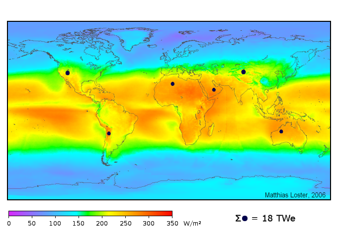
The land area needed to produce 18 terawatts (50% larger than 2010 value) using 8% efficient photovoltaics, shown as black dots. Source: WikiMedia.
We do not lack the area/resources on the planet to get enough energy from PV, even at half the current silicon efficiency. Other alternatives come nowhere close to being able to make this claim. As a side note, because North America uses 25% of the world’s energy at present, its dot may need to grow a bit, but not exorbitantly.
As reassuring as this picture is, the photovoltaic area represents more than all the paved area in the world. This troubles me. I’ve criss-crossed the country many times now, and believe me, there is a lot of pavement. The paved infrastructure reflects a tremendous investment that took decades to build. And we’re talking about asphalt and concrete here: not high-tech semiconductor. I truly have a hard time grasping the scale such a photovoltaic deployment would represent. And I’m not even addressing storage here. So while it’s physically possible, and the efficiency is sufficient to allow it, it remains a daunting challenge.
Could we even get started? Would we agree it’s the right path? Would it have much leverage against oil, given that it’s not a liquid fuel replacement? Will it always seem dreadfully expensive after being spoiled on ridiculously cheap fossil fuels? Once oil is in global terminal decline, economies will struggle to cope, and this may not seem the most opportune time to strike out on an unprecedented large-scale expenditure, whose costs and benefits will be debated hotly.
Have I ever mentioned that an easy solution is a voluntary reduction of energy demand? But this doesn’t sound like expansion/growth, so how would that idea ever gain traction?
